In the entire product journey, one step that is the most crucial and can never be overlooked is testing.
Electronics of all kinds are prone to sudden drops or shorter life spans even if they are built precisely.
PCB failure is the last thing that any manufacturer wants as it comes with significant financial losses.
PCB testing is the key to overcoming this challenge as it helps ensure quality, reliability, and, ultimately, customer satisfaction. To gain a better understanding of how PCB testing can enhance the quality of PCB products and types of PCB testing let’s deep delve into this article.
Why PCB testing is necessary and what are the benefits of PCB Testing
PCB testing plays a crucial role in the electronics industry. Without robust PCB test processes, there is a risk of not identifying defects that could potentially cause products to fail, once they’re in the market. This will result in diminished customer confidence and a poor reputation for brands.
PCB design analysis techniques can be used during the early stages to help minimize major issues during the manufacturing process, but there’s also a wide range of PCB test methods that can be used on physical boards. These printed circuit board tests, run on prototypes or small-scale assemblies, look most closely at potential shorts, solder joint issues, and functionality, ensuring that each tested PCB will function as intended.
Benefits of PCB Testing
1. Bug identification:
PCB board testing helps to catch design or manufacturing errors early on. By thoroughly testing each circuit board, manufacturers can identify manufacturability and functionality errors in the design or assembly process. This allows us to make necessary adjustments and modifications, resulting in a higher quality electronic product while preventing costly rework or product recalls.
2. Cost reduction & Time Saving:
Detecting and preventing faults in the early stage of PCB manufacturing not only increases productivity but also reduces overall production costs. Additionally, PCB test helps minimize the need for post-production repairs or replacements, saving both time and money.
3. Increased safety:
Since PCBs are used in essential electronic technologies, their defects can severely impact a company’s productivity or an organization’s critical services. A faulty PCB may even pose fire risks, endangering nearby individuals. Pre-manufacturing PCB test is crucial to prevent machinery and worker harm due to design flaws during production.
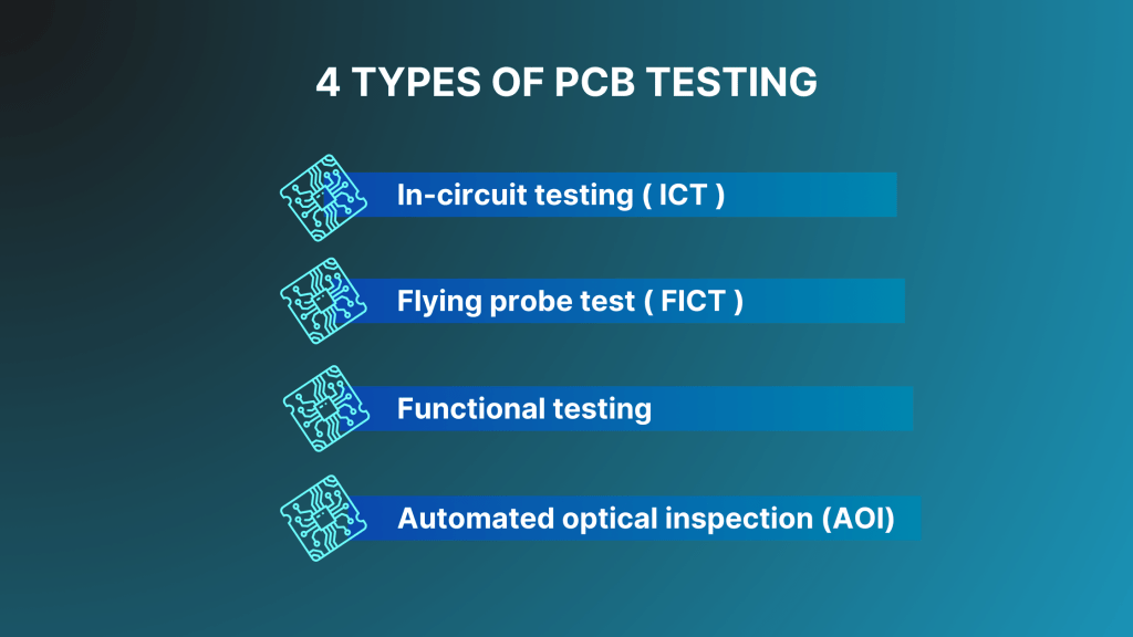
4 Types of PCB testing
PCB test methods are crucial in detecting any faults or defects that may have occurred during the manufacturing process. These methods guarantee that the PCBs meet the required performance standards, giving manufacturers and consumers the required output.
Let’s take a look at 4 common tests for PCB Testing
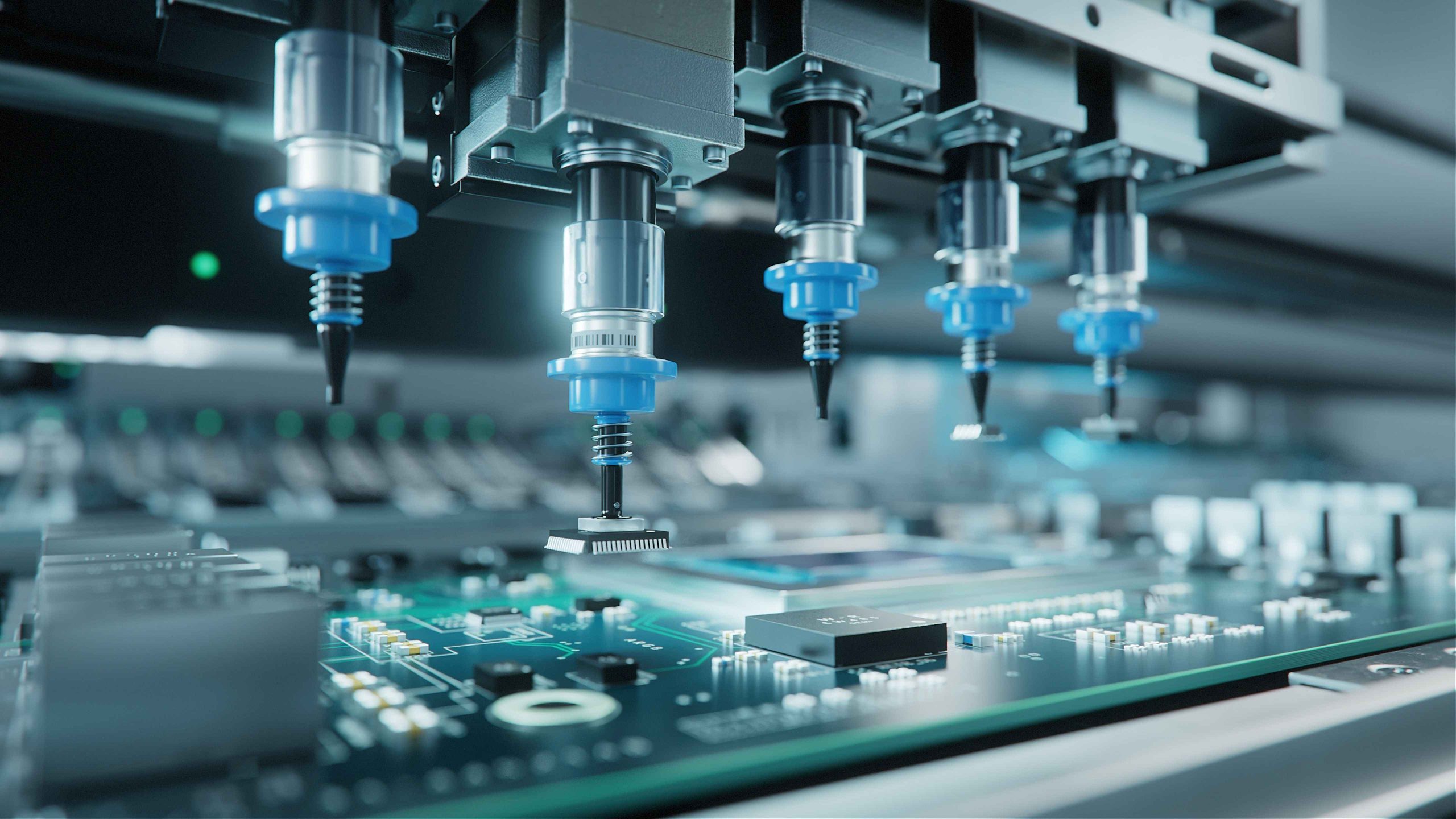
1. In-circuit testing: In-circuit testing (ICT) commonly referred to as a bed-of-nails is a high-precision method used to identify defects in individual components on the PCB to find out the hidden faults that many EMS providers prefer to employ. The PCB in-circuit test is intended for complete 100% coverage, it typically attains around 85-90% coverage. What sets it apart is that it totally eliminates human error.
In general, this PCB test method evaluates analog circuits, offering precise measurements for attributes like resistance and capacitance. It’s most cost-effective when used for the final assessment of high-volume, well-established products, but less suitable for prototypes or low-volume productions where design iterations are frequent.
2. Flying probe testing: The flying probe test, also known as the fixtureless in-circuit test (FICT), is a versatile method used in the electronics manufacturing industry for PCB testing. Unlike traditional ICT, this non-powered type test eliminates the need for custom fixtures, resulting in cost savings. PCB test fixture utilizes a basic fixture to secure the board while test pins navigate and examine relevant points on it through a program controlled by software. This PCB test excels in swift, cost-effective adaptation to new boards through simple programming adjustments.
FICT or ICT: Which one is best as per your PCB testing requirements
ICT (In-Circuit Testing) | FICT (Functional In-Circuit Testing) | |
Objective | Focuses more on physical aspects, checking for open circuits, short circuits, and component values. | Focuses on assessing functional aspects of a PCB. |
Complexity | Complex due to its detailed analysis of individual components, requiring accurate knowledge of the PCB’s layout. | Generally less complex to set up and execute, making it suitable for a variety of applications. |
Cost | Costly due to the need for sophisticated test fixtures and programming. | Cost-effective, especially for high-volume production. |
Speed | It takes longer due to the detailed component testing. | Faster test execution, making it suitable for rapid mass production |
Applicability | Ideal for component-level defects that need precise identification. | Well-suited for complex, high-density PCBs with a focus on overall system functionality. |
3. Automated Optical Inspection (AOI): Automated Optical Inspection (AOI) employs either a single 2D camera or two 3D cameras to capture images of the PCB. These images are then compared to a detailed schematic by the program. If a board doesn’t align sufficiently with the schematic, it’s marked for further inspection by a technician.
It’s crucial not to rely solely on automated optical inspection. Instead, consider using AOI in conjunction with other tests. Some effective combinations include AOI paired with flying probe testing, in-circuit testing (ICT), or functional testing. This comprehensive approach ensures robust quality control throughout the production process.
4. Functional testing: Functional testing is the final step in circuit inspection, it verifies performance by generating electrical signals and measuring their effects. The circuit is powered and stimulated via connectors, with software evaluating measurements against design specs to test PCB. This test excels at uncovering issues that emerge when the circuit is active and gauges power consumption. However, it’s costly and requires specialized, inflexible equipment often tailored to specific cards.
Some customers prefer the reliability of functional testing, but it demands external equipment, fixtures, and compliance with standards like UL and MSHA.
Time is a factor; for speedy product launches, functional testing may not be ideal. However, for quality and durability, it’s a wise investment. It ensures your product powers up reliably and meets performance and reliability standards, ultimately saving you money and preserving your reputation.
Regardless of the method chosen, the PCB test is a vital step in electronic design. As it saves time and money by detecting defects before final production.
Future Trends in PCB Testing Technology
The PCB industry is one of the fastest-growing industries. The newest trends in PCB testing are constantly evolving to make PCBs satisfy the rising demands.
Let us look at the latest trends in PCB Testing technology:
1. AI and ML Integration: PCB testing is getting smarter with the use of Artificial Intelligence and Machine Learning. They help detect defects quickly and even predict potential issues, making quality control faster and more efficient.
2. Industry 4.0 Integration: Factories are getting smarter with IoT sensors and real-time data analysis, reducing downtime and enabling quicker problem-solving.
3. Sustainability Initiatives: There’s a growing concern about the environment, even in PCB testing. People are looking into eco-friendly testing methods and using materials that are better for the planet.
Conclusion
Investing in PCB tests can improve product reliability, save manufacturers money, ensure compliance with industry standards, and speed up product development. With consumer expectations constantly rising, the PCB test is more than a best practice; it’s a necessity. As we discussed various testing methods in this blog, make sure to make the right decision as per the project’s unique needs.
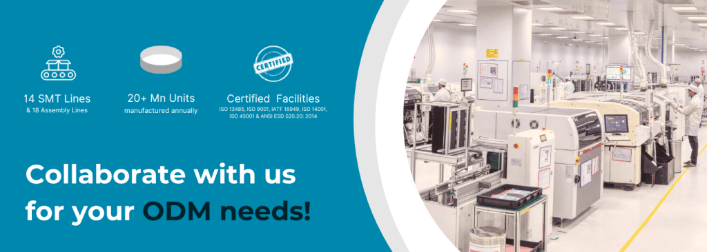
Why you should choose Napino for PCB Testing?
Cutting-edge testing: We test PCBs utilizing the latest methods of PCB testing that can be customized to suit customer needs, ensuring the devices are at the forefront of technological standards.
Pre-Certification support: With our commitment to quality we offer unparalleled pre-certification support for PCB tests.
Reliability: Choosing Napino isn’t just outsourcing testing; it’s entering into a partnership centered on precision and reliability.
Napino Digital Solutions is your reliable partner in this journey. With cutting-edge technology and unwavering commitment to excellence, we ensure rigorous and dependable testing, building trust among your customers.
So, whether you’re deciding which PCB test method to choose for your project or embracing the latest trends, remember Napino Digital Solutions – your ally in electronic excellence.